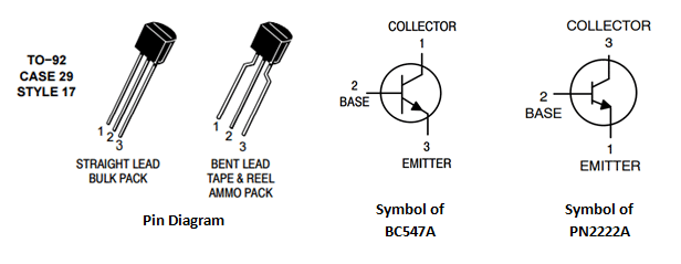
Transistor Design For Newbies
Transistors are important electronic devices that find use in a wide range of applications. Learn how to design circuits with them.
Principle of Operation
There are various analogies that you will most likely come across when first learning about transistors, a useful analogy is that of a mechanically controlled water valve.
![[insert image]](https://lunarjournal.github.io/images/3/valve2.png)
Here it is important to reference the water analogy of current and voltage. In the water analogy we picture a column of water moving through a pipe.
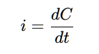
We define current as the movement of water (charge) through the pipe (wire), or in mathematical terms the rate of flow of water (charge) past a given point with respect to time:
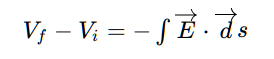
Voltage is analogous to the pressure differential between two points. For example, suppose we suspend water in a pipe and then apply a high pressure at the top and a lower pressure at the bottom. We have just set up a ‘water potential difference’ between two points and this tends to move water (charge) from the higher pressure region (voltage) to the lower pressure region. The higher the water potential, the faster the column of water (charge) moves through the pipe when it has the chance.
In reality, voltage arises due to the presence of electric fields. For a given electric field between two points, a positive test charge may be placed at any distance along the electric field lines, that is, its ‘field potential’ varies and a positive charge placed closer to the positive end of the electric field feels more repulsion (and therefore has a higher potential to do work) than at the negative end of the field.
Potential difference (voltage) is just a differential measure of this electric ‘field potential’ or put differently, the capacity of charge to do work in the presence of an electric field:
With this in mind the idea of a water valve then makes sense. The valve consists of three ports, one attached to one end of the pipe, the other port to the end section of the pipe and then the valve itself, sitting in the middle and regulating the flow of water between both ends.
By rotating the valve we adjust the water flow rate (current) through the pipe. This is the basic principle of operation of a transistor. However rather than applying a mechanical torque, we apply a potential difference at the base to regulate current flow.
You may think of the degree to which the mechanical valve is open or closed as proportional to the voltage applied at the base of the transistor. This means that we can control a potentially larger current through the transistor using a smaller current through the base (through the application of a base voltage) , this is one of the useful properties of transistors.
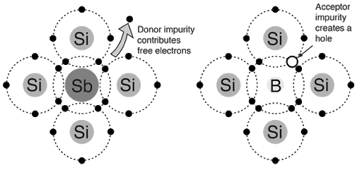
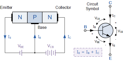
Bipolar Junction Transistors (BJTs) usually consists of three semiconductor layers which can be of two types: n or p. The individual silicon layers are crystalline structures that have what are known as dopants added to them. These are individual elements (phosphorus, boron) added to neutral silicon (and replace the corresponding silicon atoms) in order to change the electrical properties of the layer.
For example, boron [B] dopant has a valency (number of outer electrons) of 3, while silicon has a valency of 4. This means that when boron and silicon bond covalently (sharing of each others electrons) there is a mismatch (3 < 4) between their valence electrons, leaving a ‘hole’, which needs to be filled with an electron in order to match silicon’s valency. This results in a crystal structure with a net positive charge, the p type layer.
In contrast phosphorus [P] dopant has a valency of 5, again there is a mismatch (5 > 4) with silicon’s valency (4), allowing for the extra electron of phosphorus to move freely through the crystal structure and giving the overall crystal layer a negative polarity, the n type layer.
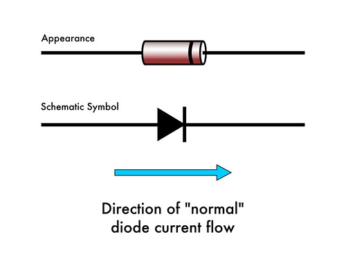
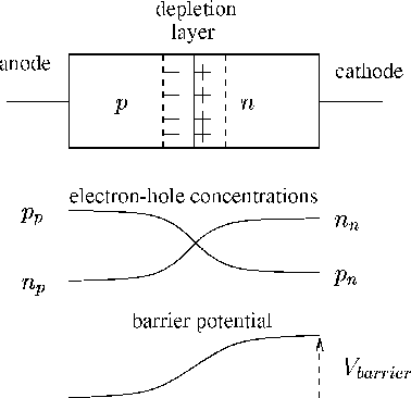
If we were to place an n region and p region together we would form an electronic device known as a diode. A diode is a 2 terminal device (with the n side connected to the negative terminal (cathode) and p side connected to the positive terminal (anode) ) that only allows current flow in one direction. It is also worth nothing that by placing an n and p region next to one another there is a localised effect at their layer boundary that results in a small number of electrons (from the n type region) migrating to the p type region in what is known as the depletion region.
The migration of electrons from the n type region to the p type region at the np boundary sets up what is known as a barrier potential, a secondary electric field at the np layer boundary in opposition to the primary E-field (between p and n).
This is the amount of voltage (pressure) required to force n layer electrons through the np barrier (the secondary E-field) where they can flow into the positive terminal (anode) of the diode.
It is equivalent to having a water valve initially shut tight and requiring a torque in order to get water flowing. A typical value for the barrier potential of garden variety diodes is between 0.3v-0.7v.
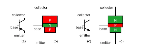
A bipolar junction transistor (BJT) may be viewed as a combination of two diodes (shown below for an NPN transistor):
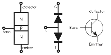
An NPN BJT transistor has two current paths, one from the collector to emitter and the other from the base to emitter. The current flow from collector to emitter represents the water flow in the pipe containing the valve, while the current flow from base to emitter represents the degree to which the valve is open or closed.
You might be wondering why conventional (positive) current flows backwards through the base-collector diode (from collector to emitter) for an NPN transistor. As it turns out, current can actually flow in multiple directions through a diode. However it takes much more voltage to ‘push’ charge through a diode in the direction it’s meant to block than in the direction it is meant to flow.
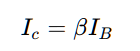
The ratio of base-emitter current to collector-emitter current is known as (β) and is an important consideration in the design of circuits using transistors:
Both transistor current paths have an associated voltage drop/potential difference across them.
For the current flow from base to emitter, there is the base-emitter voltage drop VBE and from collector to emitter there is the collector-emitter voltage drop VCE :
The values of VCE, VBE and VCB have predictable values for the three modes of operation of a transistor, these are:
- Cut-off (The transistor acts as an open curcuit; valve closed). VBE « 0.7V
- Saturation (The transistor acts as a short circuit; valve completely open)
- VBE >= 0.7V
- Active (The transistor acts as an amplifier; valve varies between closed and completely open)
Transistor as a switch
When using a transistor as a switch we place the transistor into one of two states: cut-off or saturation.
The following switching circuit is usually employed (with an NPN BJT) (shown together with an LED):
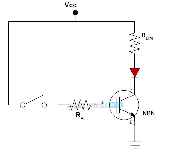
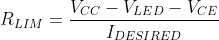
The circuit is seen consisting of a base current limiting resistor RB as well as a collector-emitter current limiting resistor RLIM.
RB serves to set up the correct base current, while RLIM serves to limit the maximum current through the LED (shown in red) when the transistor is switched fully on (driven into saturation).
To calculate the values for resistors RB and RLIM we use the equation relating base current to collector current defined earlier:
The first question becomes what collector current IC we desire. This value depends on the device/load you are trying to switch on/off. It is worth noting that when a transistor is switched fully on (is in saturation mode) the equivalent circuit (simplified) is as follows (shown without the LED, you can assume the LED follows resistor RC):
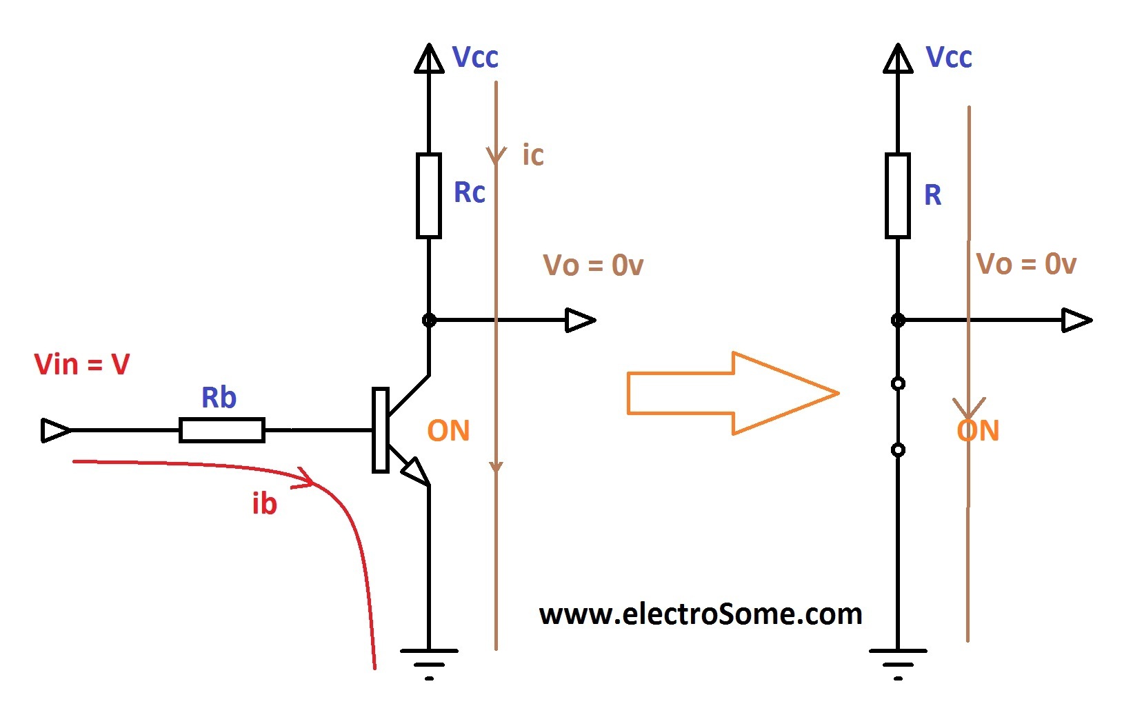
Thus at the collector a direct connection to ground is made. However this connection is not perfect and there is an associated voltage drop from collector to emitter of typically around 0.2v (VCE) rather than 0v. Determining the relevant value for IC is then just a matter how much current your load (LED in our case) requires.
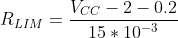
For example, a typical green led requires around 15mA of current to light up brightly so we set IC = 15mA. A green LED also typically has a 2v drop across it. To calculate RLIM we use ohms law:
Given the LED and collector to emitter voltage drops of 2v and 0.2v respectively, we can further reduce the above expression above to:
Choosing VCC is just a matter of what you have at hand. For example, a 5v or 9v supply would be adequate to drive the transistor into saturation as long as VCC » 0.7v (due to the base emitter voltage drop) and Vcc » 2v (for the led).
Assume VCC = 5v, then RLIM = 186.7 Ω
In calculating the required base current, we use the transistor’s β value. This can be found on the transistors datasheet and typically varies from anywhere between 20 to 200. The rule of thumb is to use the minimum value of β for a specific transistor type. For the standard garden variety 2N2222 transistor, the minimum value of β is around 75. Therefore to calculate IB, we have:
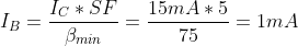
You might have noticed an additional factor called SF for (safety factor). This is a factor typically around 5-10 that we multiply our calculated IB with in order to ensure we drive the transistor into saturation. This gives a value of around 1mA for IB.
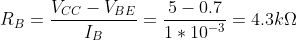
Given IB, calculating RB becomes trivial as we know the voltage across RB as: VCC - VBE (think of VBE as a 0.7v diode) and so we apply ohms law once again:
Now you can connect a switch between the base resistor and Vcc or connect the base resistor directly to the output of a 5V-TTL micro-controller in order to turn the LED on and off! The benefit of using a transistor to do that is that we require a relatively small current (<1mA) in order to switch a much larger current through the LED (15mA)!
In conclusion:
- Determine required collector current IC
- Calculate RLIM (ohms law)
- Calculate IB using lowest value for β
- Multiply IB by safety factor 5-10
- Calculate RB (ohms law)
The simple LED transistor circuit was modelled in LTSpice, with the LED represented as a series voltage source (representing the 2v voltage drop).:
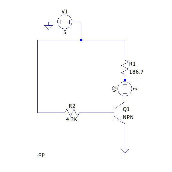
A simulation of the DC operating point of the circuit yielded:
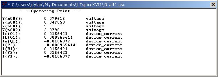
Here we can see the ~1mA base current (Ib) driving ~15mA collector (IC) current. All current values are shown in S.I units of amperes (A).
Transistor as an amplifier
Here we operate the transistor in its active mode to achieve linear amplification. Linear amplification means that our output should be a proportional scaling of our input. For example if we feed in a sine wave we should ideally get a scaled sine wave out, i.e with no distortion/clipping.
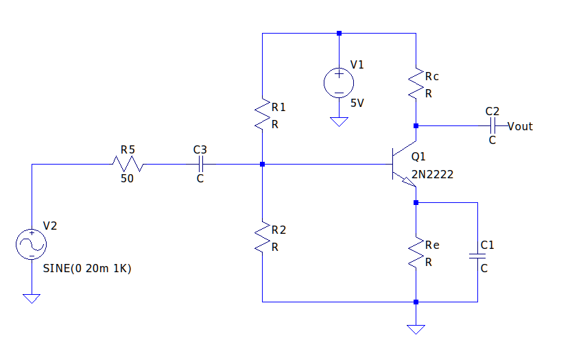
There are various circuit configurations used to achieve amplification using transistors, a useful ‘template’ is known as common emitter configuration (shown below with an NPN transistor):
Here we model a 20mVp (20mV amplitude) sinusoidal signal source with a resistance of 50 Ω, but your input can be practically anything.
It should be noted that there are two electrical ‘components’ of the above circuit, these are AC (the fluctuating component) and DC (the static component).
When analysing a circuit from a DC perspective there are a few rules to follow:
- Capacitors become open circuits
- Inductors become closed circuits
This means that at the base of Q1, C3 becomes an open connection, i.e the base of the transistor cannot see signal source V2 or the 50Ω. resistor . Additionally, capacitor C1 becomes an open circuit and therefore has no effect (it’s as if all the capacitors weren’t there in the first place).
Capacitor C3 is known as a DC blocking capacitor and is used to remove the DC component of the input signal at the feed point (base of Q1). All signals have a dc component:
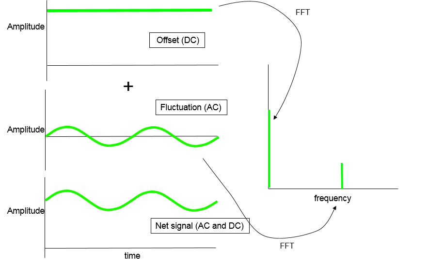
Effectively C3 serves to isolate the fluctuating(AC) component from the net signal, that is, we need a signal that moves along the line y= 0.
Capacitor C2 is also a DC blocking capacitor and also serves to remove any DC offset at the output of the amplifier.
The role of capacitor C1 is a bit more involved and requires and understanding of AC circuit analysis, specifically the AC signal gain/amplification Av which, for common emitter configuration, is given by:
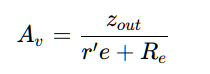
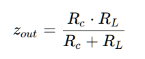
Here zout represents the output impedance of the common-emitter amplifier which is given by the parallel combination of Rc and your load resistance, RL (connected to C2).
From an AC perspective:
- Capacitors become short circuits
- Inductors become open circuits
- Voltage sources become grounds
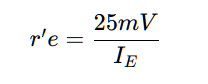
The term r’e is known as the transistor’s AC base-emitter junction resistance and is given by:
The introduction of capacitor C1 nulls out the term Re from the expression for Av. This is typically done to achieve higher values of Av than would otherwise be possible if resistor Re was still present. For lower, more controlled values of Av, resistor Re should not be bypassed by capacitor C1.
The first step in the design of the amplfier is choosing Rc such that zout isn’t affected by changes in RL. For example, for a large value of RL choose Rc « RL.
For the purposes of our example we assume RL = 100KΩ We then choose Rc = 5KΩ
Next we determine the maximum AC gain possible given a fixed zout:
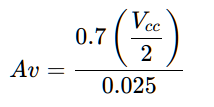
It is usually good practice to give 20% of (Vcc/2) to Re and 70% to Rc. Higher ratios of Vcc(Re) to Vcc(Rc) might lead to higher ac gain (Av) but could sacrifice operational stability as a result.
Given Vcc = 5V, we get Av = 70. This is the highest expected voltage gain for this amplifier.
We know that:
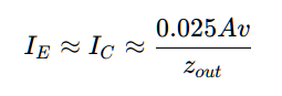
Thus, given Av = 70, zout = 5KΩ we have IE = 0.35mA. We are now able to calculate Re:
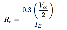
For Vcc = 5V, IE = 0.35mA we get Re =~2.1KΩ
A useful parameter for common emitter configuration is the AC input impedance (looking in from C3) and is given by:
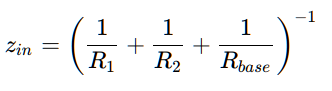
Here Rbase represents the AC input impedance of transistor Q1 (looking into the base):
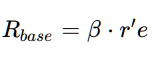
We know how to calculate r’e from earlier and we use the minimum value of β (75 for 2N2222) to calculate Rbase:
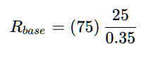
Thus Rbase = 5.4 KΩ
Returning to our DC analysis, we calculate the expected voltage at the transistor base:
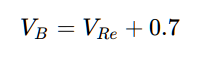
We know that VRe is 30% of Vcc/2, which gives VB = 1.45V. Now given IE = 0.35mA we can again use our minimum value for β to calculate our required base current:
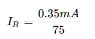
Thus IB = 4.57uA
At this point we need to ensure that small changes in the value of base current (which occur due to variations in β ) do not significantly effect the DC operating point of the amplifier circuit.
In order to ensure a stable operating point we ‘stiffen’ the voltage divider by ensuring the only a small fraction of the total resistor divider current flows into the base of transistor Q1.
A good rule of thumb is to allow for 1% of the total divider current to pass into the base of the transistor.
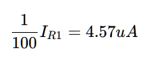
We can therefore assume that IR1 ~= IR2 and solving the above expression yields IR2 = 0.456mA. Since we know the voltage across R2 (given by VB) we can calculate the resistance value:
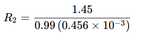
This gives R2 ~= 3.2KΩ. Finally we calculate the value of R1:
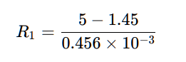
R1 ~= 7.8 KΩ
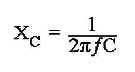
The values of capacitors C3, C2 and C1 are chosen such that the capacitive reactance (resistance at AC) at the desired signal frequency is minimal. Capacitive reactance is given by:
Now that we have all the required component values, we build the circuit in LTSpice:
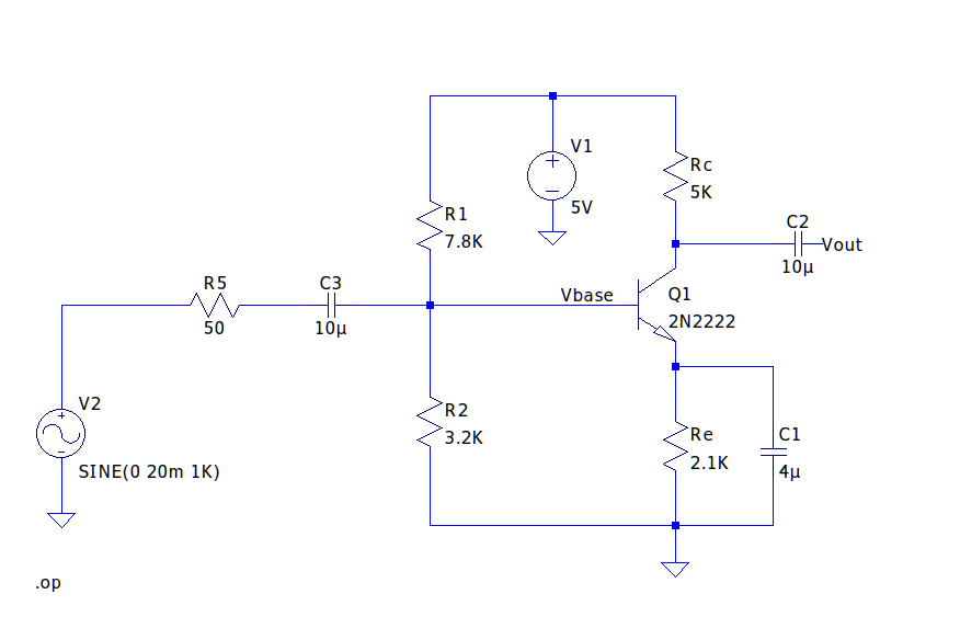
A simulation of the DC operating point was performed:
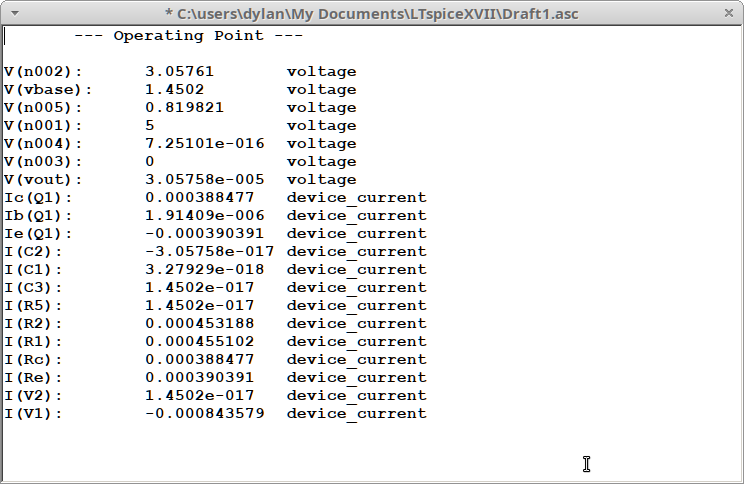
Here we can see our expected Vbase of around 1.45V and an emitter current of around 0.38mA (instead of 0.35mA), not too bad! Let’s measure the voltage gain( with the signal source set to a peak amplitude of 1mV and a 100K load attached):
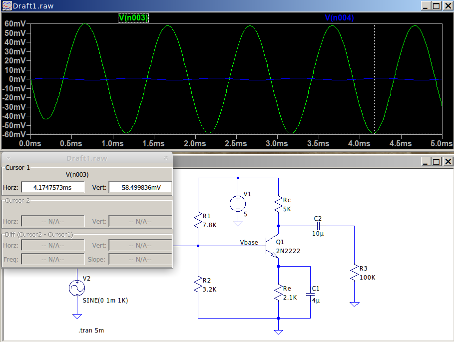
Our output across our load is seen reaching an amplitude of 60mV and so we have a voltage gain of ~60.
LTSpice
You can download LTSpice from https://www.analog.com/en/design-center/design-tools-and-calculators/ltspice-simulator.html