RF Circuit and Power Amplifier Design Basics
A short primer on some of the basic concepts related to RF circuit and RF power amplifier design.
- Average Power
- Transmission Lines
- Impedance Matching
- Electromagnetic Transducers
- S-Parameters
- Harmonic Balance
- Lumped and Distributed Element Networks
- Classes Of Operation
- Stability Analysis
- Efficiency
- P1dB Compression Point
- Load Pull
- LC Filtering
Foreword
The aim of this journal entry is to review some basic technical concepts pertaining to general RF circuit design and modelling as well as RF power amplifier design.
RF circuit design is typically not covered in detail at an undergraduate level and the author hopes that this journal entry will provide some useful information to readers not familiar with the subject.
RF Transmission and Reception
Average Power
In order to be successful in RF power amplifier design, it is necessary to understand AC power from both a frequency and time domain perspective.
In the frequency-domain, complex AC power (\(S\)) is given by:
\[S = \overline{V}.\overline{I}^*\]Where \(\overline{V}\) and \(\overline{I}\) are the voltage and current phasors. In RF power amplifier design we are typically concerned with maximizing the real component of complex power \(\Re(S)\) which represents power dissipated in a load such as an antenna (modelled by it’s radiation resistance). The imaginary part of \(S\) represents reactive power which does not perform any useful work.
Average real power (\(P_{avg}\)) is the industry standard measure of power for RF and microwave systems and is measured in the SI units of Watts (W). Average power over total time (\(T\)) for a continuous-wave (CW) signal is defined by the following time-domain integral:
\[P_{avg} = \frac{1}{T} \int\limits_0^T v(t).i(t) dt\]The terms \(v(t)\) and \(i(t)\) can then be expanded:
\[v(t) = v_{p}sin(2\pi ft), i(t) = i_{p}sin(2\pi ft + \theta)\]Here \(\theta\) represents the phase angle between \(i(t)\) and \(v(t)\) and (\(v_{p}\)) and (\(i_{p}\)) represent the peak values of the voltage and current waveforms.
It can be shown that for purely sinusoidal voltage and current waveforms:
\[P_{avg} = \frac{1}{2}v_{p}i_{p}cos(\theta)\]Hence maximum real power is obtained when the current and voltage waveforms are in phase. \(cos (\theta)\) is commonly referred to as the power factor and this constant relates real power to apparent power \(\|S\|\). Apparent power is the total complex power available to a particular load.
In practice average real power is specified in terms of decibels referenced to 1 milliwatt (\(dBm\)):
\[dBm(P) = 10\log_{10}(\frac{P}{1mW})\]While relative power is measured in decibels (\(dB\)):
\[dB(P) = 10\log_{10}(\frac{P}{P_{ref}})\]Transmission Lines
Traditional lumped circuit theory is only applicable to low frequency circuits as it assumes that wires are lossless with negligible electrical length. Electrical length is usually measured in terms of multiples of the wavelength (\(\lambda\)) of the highest frequency signal that is conducted over the line.
As a rule of thumb, when the length of a wire is greater or equal to \(\lambda/10\), the voltage and current in the wire as a function of position along the wire will no longer be constant with time and wave-like behaviour such as reflection and standing waves start becoming important. In these cases utilizing a distributed model, such as the transmission line, often becomes necessary.
Let \({u}\) and \({i}\) represent the voltage and current along the transmission line as a function of position and time:
\[u = u(x,t), i = i(x,t)\]Then at distance \({x+dx}\) voltage and current can be expressed with a taylor series expansion:
\[u(x + dx) = u(x,t) + \frac{\partial u}{\partial x} dx\] \[i(x + dx) = i(x,t) + \frac{\partial i}{\partial x} dx\]A segment of a traditional transmission like is shown in the figure below. It consists of a series distributed resistance \(R(x)\), inductance \(L(x)\) as well as segment capacitance \(C(x)\) and conductance \(G(x)\). A transmission line is thought of as a continuous series of these segments.
![]()
It can be shown that the equations that describe changes in the voltage and current on the line is given by:
\[\frac{\partial u}{\partial x} dx = -Ri - L \frac{\partial i}{\partial t}\] \[\frac{\partial i}{\partial x} dx = -Gu - C \frac{\partial u}{\partial t}\]The equations above are known as the telegrapher’s equations. These two equations can be combined to produce two partial differential equations with one isolated variable each (\({u}\) or \({i}\)).
\(u\) and \(i\) are related by the characteristic impedance (\(Z_{0}\)) of the transmission line which can be derived from the telegraphers equations:
\[Z_{0} = \frac{V^+(x)}{I^+(x)} = \sqrt{\frac{R(x)+j\omega L(x)}{G(x)+j\omega C(x)}}\]For most transmission lines dielectric and conductor losses are low, so we assume:
\[R(x) \ll j\omega L(x), G(x) \ll j\omega C(x)\]As a result the equation above simplifies to:
\[Z_{0} = \sqrt{\frac{L(x)}{C(x)}}\]It is worth noting that characteristic impedance \(Z_{0}\) of a transmission line only has an effect at RF frequencies. It is not possible to measure the characteristic impedance of a transmission line directly with a multimeter because resistance (ohms law) and characteristic impedance (electromagnetic property) are not the same concept.
Examples of transmission lines include coaxial cable and microstrip line. Transmission lines typically have a characteristic impedance of 50 \(\Omega\) in RF systems and are used to carry RF signals from one point in a circuit to another with minimal losses.
Impedance Matching
It is often said that impedance matching is what truly differentiates RF circuit design from low frequency circuit design. Indeed, it is one of the most common tasks for an RF designer.
RF signals travelling along a transmission line can be thought of as electromagnetic power waves. Power waves are a hypothetical construct, one of the many possible linear transformations of voltage and current.
The figure below shows a typical RF circuit consisting of a RF power source (\(G\)) with an impedance of (\(Z_{R}\)) and a load with an impedance of \(Z_{L}\). The interface of the generator and load impedance is indicated by the dotted line.
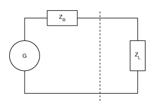
It is at this interface that we experience reflection of the power wave (back to the generator) when \(Z_{R} \neq Z_{L}\). If the impedance of the generator and load were equal then no reflection occurs.
In general, the goal of an RF system is to transfer RF power as efficiently from one point to another with minimal reflections. The degree of an electromagnetic power wave reflected (at the boundary) is determined by the reflection coefficient (\(\Gamma\)):
\[\Gamma_{L} = \frac{Z_{L} - Z_{0}}{Z_{L}+Z_{0}}\]A \(\Gamma\) of \(0\) indicates no reflection, while a \(\Gamma\) of 1 or -1 represents total reflection with or without phase inversion.
Here (\(Z_{0}\)) represents the reference impedance of the system which is typically \(50 \Omega\). Maximum power transfer over the boundary from the generator to the load is only satisfied when:
\[Z_{L} = Z_{R}^*\]This expression is known as the conjugate match rule for maximum power transfer. In most practical RF systems \(Z_{L} \neq Z_{R}\) and so a method of impedance transformation is required to satisfy the conjugate match rule.
Impedance transformation networks allow a \(Z_{L}\) with both a real and imaginary part to be transformed into another complex impedance using reactive components. Reactive components do not dissipate real power unlike resistors which is why resistors are rarely used in RF impedance matching and filter networks.
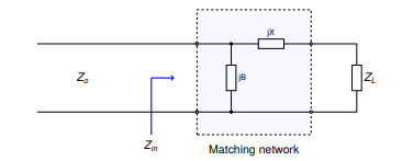
The most basic type of impedance transformation network is known as the LC network which consists of an inductor and capacitor. It can be used to transform a complex load (\(R_{L}\)) to 50 \(\Omega\). The figure below shows the basic configuration of the LC impedance transformation network.
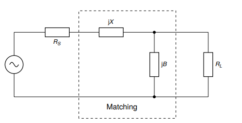
In addition to the LC network’s impedance transformation property, the LC network can have a low-pass or high-pass response depending on the shunt element (\(jB\)). If it is capacitive then the LC network will have a low-pass response or a high-pass response if it is inductive.
Typically the low pass configuration (with a shunt capacitor) is desired.
It should be noted that the shunt element (\(jB\)) should be placed on the side with the largest impedance. Therefore there are two possible configurations of this network:
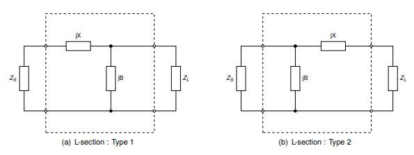
So that type 1 is used when \(R_{L} > R_{S}\) and type 2 is used when \(R_{L} < R_{S}\). Here \(Z_{S}\) represents \(Z_{0}\) the system reference impedance \((50 \Omega)\).
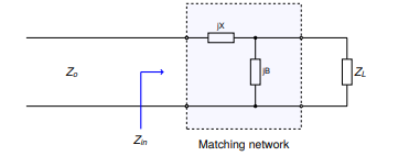
The design procedure for a type 1 LC network is as follows. First we evaluate the input impedance (\(Z_{in}\)) looking into the matching network.
We start by defining a few variables. Let:
\[Z_{L} = R_{L} + jX_{L}\] \[Z_{S} = Z_{0} = 50 \Omega\] \[Z_{in} = jX + \frac{1}{(jB)^{-1} + (Z_{L})^{-1}}\]Matching conditions are met when \(Z_{in} = Z_{S} = Z_{0}\).
The equation above can be simplified and separated into real and imaginary parts:
\[B(X + X_{L}) = -(Z_{0}R_{L}-XX_{L})\] \[B(R_{L} - Z_{0}) = Z_{0}X_{L} - R_{L}X\]B can then be solved using the following equation:
\[B = -\frac{R_{L}^2+X_{L}^2}{X_{L} + \sqrt{\frac{R_{L}}{Z_{0}}} \sqrt{R_{L}^2 + X_{L}^2 - Z_{0}R_{L}}}\]Once B is obtained, X may be found by rearranging for X:
\[X = \frac{B(R_{L} - Z_{0}) - Z_{0}X_{L}}{-R_{L}}\]The figure below depicts the second variant of the LC matching network.
Let:
\[Z_{L} = R_{L} + jX_{L}\] \[Z_{S} = Z_{0} = 50 \Omega\] \[Z_{in} = \frac{1}{(jB)^{-1} + (Z_{L} + jX)^{-1}}\]Matching conditions are met when \(Z_{in} = Z_{S} = Z_{0}\).
The equation above can be simplified and separated into real and imaginary parts:
\[B(X_{L} + X) = -Z_{0}R_{L}\] \[B(Z_{0} - R_{L}) = -Z_{0}(X_{L}+X)\]Again, B can then be solved using the following equation:
\[B = -Z_{0}\sqrt{\frac{R_{L}}{Z_{0}- R_{L}}}\]Again, X may be found by rearranging for \((X_{L} + X)\) and substituting to yield:
\[X = \sqrt{R_{L}(Z_{0} - R_{L})} - X_{L}\]For both LC circuit types it is assumed that \(jB\) represents a capacitive element and \(jX\) represents an inductive element so that a low-pass response is obtained.
Matching networks with more than two reactive elements also exist. These include the \(\pi\)-section and T-section matching networks that contain 3 reactive elements each. The figure below depicts the \(\pi\)-section network.
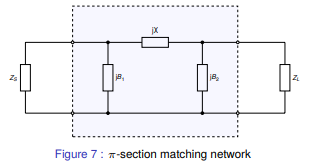
The \(\pi\)-section network is made up of a type 2 LC matching network in cascade with a type 1 LC matching network. The central element \(jX\) is the sum of the inductive reactance (\(jX\)) of each LC matching section, which is combined into a single reactance.
A virtual load resistance \(R_{x}\) is interposed in-between the two LC matching networks. The goal of the first LC matching network is to then match the source \(Z_{S}\) to \(R_{x}\) while the second LC matching network matches \(R_{x}\) to \(Z_{L}\).
The value of \(R_{x}\) is chosen according to the desired Q-factor and must be smaller than \(R_{L}\) and \(R_{S}\). The Q-factor of a matching network describes how well power is transferred from source to load as you deviate from the designed center frequency of the matching network (\(f_{0}\)). Is it defined as follows:
\[Q = \frac{f_{0}}{B}\]Here \(f_{0}\) represents the center frequency of the matching network and B represents the total bandwidth over which no greater than 3dB of power is lost from source to load.
A high Q-factor is often desirable for a broadband matching network. It should be mentioned that the Q-factor cannot be controlled with a simple 2 element LC matching network (which id determined by \(R_{L}\) and \(R_{S}\)). This is one of the advantages of the \(\pi\)-section matching network.
The Q-factor for the \(\pi\)-section filter is given by:
\[Q_{\pi} = \sqrt{\frac{\max(R_{S}, R_{L})}{R_{x}} - 1}\]Here \(\max()\) is a function that returns the maximum of two values. Hence the Q-factor of a \(\pi\)-section matching network will be determined by the LC matching section with the highest Q-factor.
Electromagnetic Transducers
Once the necessary RF power has been generated and transmitted over various transmission lines and matching networks it then becomes necessary to convert this RF power into electromagnetic waves which can start propagating through free space to reach a receiver. For this purpose we use an electromagnetic transducer known as an antenna.
An antenna can be also be thought of as an impedance transformation network that matches an RF circuit (50 \(\Omega\) typical) to free space (377 \(\Omega\)).
An antenna can be as simple as a piece of wire connected to an RF output port but the efficiency of the antenna in this case would be very low. The two most common types of antenna’s are the monopole and dipole antenna (shown below).
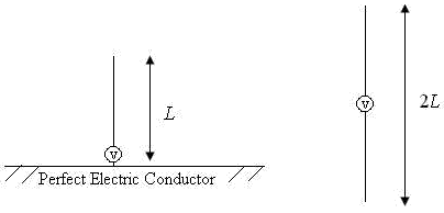
The monopole antenna consists of a quarter-wave length (\(\lambda/4\)) of wire of length \(L\) which is connected to the ‘hot’ RF input terminal and a infinitely large RF ground plane conductor which is connected to electrical ground. The ‘hot’ and RF ground elements are electrically separated from each other.
Most practical HF and VHF monopole antennas are shorter than a quarter wavelength due to size constraints and are therefore modelled as electrically small monopoles (\(L \leq (1/8)\lambda\)) from this point forward.
An electrically small monopole antenna can be modelled as a series circuit with the elements shown in the image below.
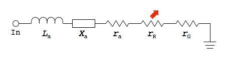
\(L_{a}\) represents the antenna conductor inductance. This is the parasitic inductance of the active element of the antenna which is just a wire made out of a material such as copper with a length and diameter. This value is usually very small and can be neglected.
The reactance of an electrically short monopole (\(L \leq (1/8)\lambda\)) is represented by \(X_{a}\) and can be calculated as follows:
\[X_{a} = 60(1 - \ln{(\frac{L}{a})})\cot{(2\pi\frac{L}{\lambda})}j \Omega\]This equation originally appears in the “Antenna Engineering Handbook”, Third Edition by Richard C. Johnson.
From the equation above it can be seen that the reactance of an electrically short monopole is primarily capacitive.
The radius of the wire (active element) in meters is given by \(a\) and the operational wavelength is given by \(\lambda\). The operational wavelength can be calculated by the transmit frequency (\(f_{t}\)) and the speed of light in a vacuum (\(c\)):
\[\lambda = \frac{c}{f_{t}}\]The loss resistance \(r_{a}\) is the effective ac resistance of the antenna active element due to the skin effect. The skin effect is a phenomenon whereby RF current tends to flow near the surface of the conductor as the frequency, and as a consequence, magnetic field strength at the center of the conductor increases.
The skin depth is given by:
\[\delta = \frac{1}{\sqrt{\pi f_{t} \mu_{0} \sigma}}\]\(\sigma\) is the conductivity of the active element’s composite material (copper) while \(\mu_{0}\) is the permeability constant. Once \(\sigma\) is computed the real ac resistance can be found as follows:
\[r_{a} = \frac{L}{2\pi a \delta \sigma}\]At VHF the loss resistance \(r_{a}\) is also very small and can typically be neglected.
The radiation resistance \(r_{R}\) of an electrically small monopole (\(L \leq (1/8)\lambda\)) is the effective real resistance that represents the power that is radiated away from the antenna as electromagnetic waves. For an electrically short monopole, radiation resistance is given by the equation below:
\[r_{R} = 40 \pi^2(\frac{L}{\lambda})^2 \Omega\]\(r_{G}\) represents the losses in the RF ground plane and this parameter is usually neglected. A stable RF ground plane is essential for an antenna to function correctly. An antenna ground plane serves as an RF return path for AC displacement current.
For a monopole the ground plane also serves the function of mirroring the active radiation element to form the second half of the antenna. This derivation is obtained using image theory and is beyond the scope of this dissertation.
RF Network Simulation Techniques
S-Parameters
Most passive RF circuits such as filters, matching networks, etc are linear. That is their output voltage, current and power relationships are derived from a system of linear equations. Some active devices such as class-A small-signal amplifiers are also linear.
Scattering parameters or S-parameters can be used to model the behaviour of these linear RF networks when stimulated by a steady-state signal.
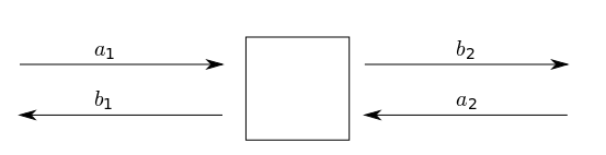
The image above depicts a DUT ‘black box’ which we use to derive the scattering parameters. The network has 2 distinct ports (port 1, port 2) and 4 scattering parameters: \(S_{11}, S_{12}\) and \(S_{21}, S_{22}\). The scattering parameters are complex values with both a real and imaginary part.
We define each scattering parameter in terms of two voltage waves at the input (port 1) and output (port 2). Let \(a_{1}, b_{1}\) represents the incident and reflected voltage waves at port 1 while \(a_{2}, b_{2}\) represent the incident and reflected voltage waves at port 2. The S-parameters can then be defined as follows:
\[S_{11} = \frac{b_{1}}{a_{1}} = \frac{V_{1}^-}{V_{1}^+}, S_{12} = \frac{b_{1}}{a_{2}} = \frac{V_{1}^-}{V_{2}^+}\] \[S_{21} = \frac{b_{2}}{a_{1}} = \frac{V_{2}^-}{V_{1}^+}, S_{22} = \frac{b_{2}}{a_{2}} = \frac{V_{2}^-}{V_{2}^+}\]It should be mentioned at this point that s-parameters can also be defined in terms of ‘power waves’ by considering the complex input impedance of the DUT. However the voltage wave definition is the most popular.
A system of linear equations can then be derived for \(b_{1}\) and \(b_{2}\):
\[b_{1} = S_{11}a_{1} + S_{12}a_{2}\] \[b_{2} = S_{21}a_{1} + S_{22}a_{2}\]Which can be expressed in terms of the S-parameter matrix:
\[\begin{bmatrix} b_{1} \\ b_{2} \end{bmatrix} \begin{bmatrix} S_{11} S_{12} \\ S_{21} S_{22} \end{bmatrix} = \begin{pmatrix} a_{1} \\ a_{2} \end{pmatrix}\]There are various useful definitions that can be derived from the scattering parameters. \(S_{21}\) and \(S_{11}\) are the most commonly used scattering paramters.
The first useful definition is the logarithmic power gain of the network in dB (\(G_{p}\)) which can be expressed in terms of \(|S_{21}|\):
\[G_{p} = 20\log_{10}|S_{21}|\]\(S_{11}\) is related to the input reflection coefficient \(\Gamma_{in}\) and can be used to obtain the input impedance of the network \(Z_{in}\):
\[S_{11} = \Gamma_{in}\] \[Z_{in} = Z_{0} \frac{1+S_{11}}{1-S_{11}}\]The ratio of reflected (\(P_{ref}\)) and incident power (\(P_{inc}\)) at port 1 is given by:
\[\frac{P_{ref}}{P_{inc}} = |\Gamma_{in}|^2\]Another useful definition is the input (port 1) return loss \(RL_{in}\):
\[RL_{in} = -20\log_{10}(|S_{11}|)\]From the above formula it can be seen that return loss is typically a positive number (since \(|S11| < 0\)), however sometimes it is quoted as a negative number in which case the data is referring to the log magnitude of \(S_{11}\) directly (\(-RL_{in}\)), not the actual return loss which is positive as mentioned.
Return loss for (\(S_{11}\)) is a measure of how well matched port 1 of the network is to the reference impedance. A return loss greater than 10dB is usually desirable for a good match.
Another measure of how well matched a network is to the reference impedance is called VSWR (voltage standing wave ratio). The VSWR of port 1 (\(s_{in}\)) is defined by:
\[s_{in} = \frac{1+|S_{11}|}{1-|S_{11}|}\]VSWR is typically used to measure the matching conditions of antennas. A (\(s_{in} < 2\)) is generally considered suitable for most antenna applications.
A VNA (Vector Network Analyzer) is an instrument that is used to measure S-parameters. Most affordable commercial VNA’s are 2-port 1-path devices, i.e they only measure \(S_{11}\) and \(S_{21}\) and the DUT must therefore be reversed to obtain \(S_{22}\) and \(S_{12}\).
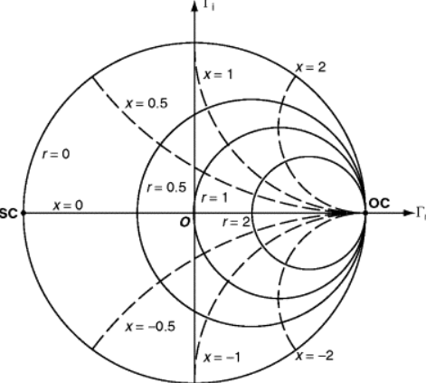
The input and output impedance obtained for \(S_{11}\) and \(S_{22}\) can also be represented in graphical form as a smith chart. A smith chart is a real and imaginary chart where the imaginary (y-axis) axis has been bent around the x-axis. It can be used to plot any value of complex impedance. An example of the Smith Chart is shown in the figure below.
The top half of the smith chart represent inductive reactance while the bottom half represents capacitive reactance. The circles passing through the x-axis are known as constant resistance circles where the left most point on the real axis of the smith chart represents a short circuit (SC) while the rightmost point represents an open circuit (OC).
For an ideal \(50 \Omega\) match there should be a single point in the middle of the smith chart.
Harmonic Balance
RF power amplifier’s are large-signal non-linear devices.
At this point a distinction is required between small signal and large signal amplifiers. For small-signal amplifiers the input and output power is typically small and these devices typically operate in their linear region.
Large-signal, class AB, B and C devices typically operate with large input and output power and their response is strongly non-linear due to the class of operation. Therefore for power amplifier classes other than class A, S-parameters cannot be used reliably in the design of RF power amplifiers.
Rather a designer relies on vendor supplied non-linear software models of the power amplifier transistor and typically uses a non-linear frequency domain analysis technique such as the harmonic balance method (HBM) to characterise the power amplifier’s performance.
Harmonic balance is a frequency domain technique used to calculate the steady state response of a non-linear circuit. HBM can be defined in multiple ways, however in this case let us demonstrate HBM through an example circuit.
Given a circuit with \(N\) nodes, let vector \(v\) represent the respective node voltages. For ease of representation we model a circuit with capacitors and voltage controlled resistors. Then applying KCL (Kirchoff’s Current Law) to the circuit yields the following systems of equations:
\[f(v,t) = i(v(t)) + \frac{d}{dt}q(v(t)) + \int_{-\infty}^t{y(t-\tau)v(\tau)} + i_{s}(t) = 0\]We let \(q\) and \(i\) represent the sum of the charges and currents entering the nodes due to the non-linearities. \(y\) is the impulse response matrix of the circuit with all non-linearities removed while \(i_{s}\) represents the external source currents.
We then convert equation above into the frequency domain:
\[F(V) = I(V) + ZQ(V) + YV + I_{s} = 0\]Here \(Z\) represents a matrix with frequency coefficients representing the differentiation step. The convolution integral in the equation above maps to YV as shown where Y is the admittance matrix for the linear portion of the circuit.
V then contains the fourier coefficients of the voltage at each \(N\) nodes at every harmonic. This process is merely nothing more than KCL in the frequency domain for non-linear circuits.
Various circuit simulators such as Keysight’s ADS (advanced design system) support the harmonic balance method (HBM).
Lumped and Distributed Element Networks
As mentioned above, as the size of a circuit element starts to approach a fraction (typically 1/10) of the wavelength of the highest RF signal frequency, the lumped element approximation for the circuit element no longer holds. In these cases lumped or discrete components cannot be used and so a distributed element/model must be utilized.
Traditionally the use of lumped element components at RF frequencies is most common below around 500 MHz. Above 500MHz these lumped circuit elements become more difficult to design with.
RF Power Amplifier Design
Classes Of Operation
Depending on the DC operating point of the power transistor, different values of efficiency and output power can be obtained for the same input power. Efficiency is generally considered the most important design parameter for an RF power amplifier.
In the class-A configuration the transistor is biased such that the quiescent drain current is equal to the peak amplitude of the current expected through the load. This allows for a symmetrical voltage and current swing at the output and the transistor conducts for the full 360 degrees of the input waveform.
The advantages of this configuration are excellent linearity and gain at the expense of reduced efficiency. A class-A power amplifier with an inductively loaded drain has a maximum theoretical efficiency of 50%.
Class-B power amplifiers aim to achieve greater efficiency by only conducting for half of the input drive cycle (180 degrees). Class-B power amplifiers have a maximum theoretical efficiency of 75 % and the transsitor is biased at cutoff. Again class-B PA’s can be placed in a single-ended configuration or push-pull. The advantage of class-B are increased efficiency at the expense of decreased linearity.
A compromise is thus needed between class A and class B such that we have sufficient linearity at a reasonable efficiency. A Class-AB power amplifier is a solution to this problem.
In the class-AB mode of operation the transistor is biased with a quiescent drain current slightly to moderately above cutoff, depending on the linearity requirements. This improves the linearity of the power amplifier while typically maintaining an efficiency of 50% to 70% in practice. Class-AB power amplifier’s have a conduction angle between 180 and 360 degrees.
The single-ended, class-AB mode of operation is therefore a popular choice amongst designers.
Stability Analysis
RF power amplifier’s are inherently unstable devices which often require some form of stabilization to operate correctly.
Amplifier instability is usually caused by some type of gain and feedback mechanism. In MOSFET transistor’s the feedback mechanism is typically due to the gate to drain capacitance that couples a portion of the output back into the input and vice versa. This effect often manifests as unwanted oscillation at either the input and output of the PA.
Small signal parameters (such as S-parameters) are typically used to characterize stability of RF power amplifier’s even though these are non-linear devices. This is because small signal models can still provide useful insights into the design of a PA without requiring complex non-linear calculations. Typically the operation of a PA is linearized around an operating point.
There are various stability factors available to a designer and an amplifier may be conditionally stable or unconditionally stable. If an amplifier is conditionally stable then there exists a load and source impedance that causes the amplifier to oscillate. Therefore unconditional stability is usually desired.
The most common stability factor in use is the Rollet stability factor (\(K\)) which is defined as follows:
\[K = \frac{1 - |S_{11}|^2 - |S_{22}|^2 + | \Delta |^2}{2|S_{12}S_{21}|}\]Here \(\|\Delta\|\) is defined as the scattering-matrix determinant:
\[| \Delta | = |S_{11}S_{22} - S_{21}S_{12}|\]We define three more stability Criterion in terms of \(\Delta, B_{1}\) and \(B_{2}\):
\[B_{1} = 1 + |S_{11}|^2 - |S_{22}|^2 - |\Delta|^2\] \[B_{2} = 1 + |S_{22}|^2 - |S_{11}|^2 - |\Delta|^2\]In order for an amplifier to be conditionally stable we require the following conditions:
\[K \ge 1\] \[\Delta < 1\] \[B_{1} > 0, B_{2} > 0\]Support for simulating these stability factors is common in most professional RF circuit design software such as Keysight’s ADS (Advanced Design System).
Efficiency
The most common measure of RF power amplifier efficiency is \(PAE\) (power added efficiency) and is defined as follows:
\[PAE = \frac{P_{out} - P_{in}}{P_{DC}}\]Here \(P_{in}\) represents the RF input power from the source, \(P_{out}\) represents RF power delivered to the load and \(P_{DC}\) represents the total DC power.
P1dB Compression Point
The P1dB point is defined as the output power level at which the gain of an amplifier decreases by 1 dB from its nominal value which indicates the onset of gain non-linearity.
Most amplifier’s start to compress approximately 5 to 10 dB below their P1dB point.
The P1dB point indicates that power amplifier’s have a linear and non-linear region of power gain as shown in the figure below.
Load Pull
Load-pull is an empirical RF PA design technique in which the reflection coefficient or impedance presented to the drain of a RF power transistor is varied by an electrical or mechanical impedance tuner to any arbitrary value. The technique is traditionally used to determine the optimum load impedance to present to an RF power amplifier for maximum output power.
Once the optimum load impedance is determined the synthesis of matching networks can then take place. Load-pull tuners are expensive devices and are therefore typically out of the reach of most students or experimenters.
In the case where a physical load-pull tuner is not available and a non-linear model for the chosen RF power transistor exists, then a simulated load-pull can be performed. Various RF CAD tools support load-pull simulations such as Keysight’s ADS (Advanced Design System).
LC Filtering
As non-linear devices, power amplifiers typically produce harmonic frequency content that must be filtered out in order to comply with regulatory standards on spurious emissions. LC networks can be constructed with varying number of elements (poles) in order to achieve a specific roll-off in the stop-band.
Two types of filter response are commonly used in RF circuit design, these are the Chebyshev and Butterworth responses. Chebyshev LC filters typically have a steeper roll-off but suffer from passband ripple.
Butterworth LC filters typically have a flat response in the passband with a gradual roll-off in the stop band. These types of filters can be designed manually using filter constants or using RF design software such as Matlab (RF Toolbox) and typically an optimization algorithm. We typically optomize for either stopband attenuation or input impedance.